DIY : Making your own Metal Core Printed Circuit Boards for led applications .

stardustsailor

Well-Known Member
Now ...

Parts /Tools /Raw materials /etc that are necessary :

-Metal core pcb prototyping sheet ...
( Alum thickness : 0.9-1.5 mm . Insulation layer thickness : 30-100 um . Copper thickness : 50-150 um )
Somewhat ,still kinda tricky to obtain ....Search the web ..Or big electronic supplies stores ...

I found the ones I use , pretty easy at a local store : mcpcb raw 1.jpg.....
I know that are fabricated and imported from Germany or Austria ..
Unfortunately ,I do not know the brand ...
But they are of really high quality ..Tested to their extremes ....


- B/W laser printer ..1200 dpi resolution is more than fine .

- Cheap semi-glossy paper & A4 simple paper

-Etching agent .Sodium Persulfatefor this purpose is very good ...

-Scotch-brite ( or similar ) green hard sponge

-Acetone

-Black markers ( some fine tipped ,some with thicker tip)

-Pyrex (deep/wide ) bowl

-wooden chopsticks

-Clothing Iron

-PCB design software ( freeware edition of i.e DipTrace )

-Table saw .

-Small file set & fine sandpaper ( # 1000- 2500 )
 

stardustsailor

Well-Known Member
Afterwards ,when crucial decisions have been taken ..

( Type / numer of leds used ...Their arrangement ...Cooling calculations ...Light cone calculations ...etc ... )

First a pcb design has to be made ....

For that ,a pcb design software is needed ..(Personally, I use DipTrace )...

There ,according to led's maker suggestions/guide notes / solder pad dimensions , a " pad " has to be designed first ....

More or less ,is a "stamp " which is the led's solder power & thermal solder pads ...

In case of tiny ceramic leds ,dimensions are really small ...Set the "raster " at least at 0.05 mm

Follow makers suggestions/guide notes / solder pad dimensions,as close as possible ...
....
( In case of different leds used ,then for every type of led ,a "pad stamp " has to be made first .. )

Afterwards ,using the "pad stamp " ,a whole circuit can be designed ,with help of
Ruler tool , Thermal copper pouring ,manual or auto tracing ,etc ...
Starting like that ....working enviro.jpg


To end up to something like that ===> 705x591_300dpi_mcpcb.jpg....
 

stardustsailor

Well-Known Member
.....

Then on to printing .....

Set the printer at his best quality ,max sharpness and /or contrast ,heavy toner deposition ( " thick/printed paper " ) .....

You 'll need to find the right "transfer " paper ...
For me cheap -free- leaflets /catalogs from Super Markets /IKEA/etc has worked best ...
Paper has to be kinda rubberish and semi-glossy ...Kinda waxy ...

Cut a piece smaller than A4 size ...
Place it over a simple A4 plain sheet of paper ...(the "carrier " ... )
(At center ...)

With Selotape ,secure it ,at the side that enters the printer first ....

Place it on printer ....Hit " print " button ...

P4196485.JPG
 

stardustsailor

Well-Known Member
Now ...Preparing the mcpcb for thermal transferring ...

Better to be pre-cut in their final size....

Mcpcb sheet has two plastic films ,protecting the alum. base and the copperside ,respectively ...

After pcb is cut in size ,remove the top film ,protecting the copperside ...

Using the green scotch-brite sponge (dry as is ) ,scrape/clean thoroughly the copperside ,until copper "shines " bright ..
Use a linear back'n'forth motion ..Avoid circular motions ...

P4196486.JPG...

When pcb is brushed enough ,with a clean paper towel dipped with acetone ,clean
carefully the copperside ....

Caution : Until the print is placed on the pcb ,no fingerprints ,fat,dust or other dirt / contamination has to exist / form in the just processed ,clean & fat-free copperside ...


Cut carefully the print to be transferred ,as close to it's borders ..

Place mcpcb on a hard wooden or other heat-resistant surface .
Copper side facing upwards ...

Place it over the copperside of pcb ,carefully (toner print to facing copperside,of course..)..
Adjust /align ,so to sit correct ....

Place a dry paper towel over pcb ...
Set clothing iron toit's max setting ...
Place ,iron over towel to pre-heat pcb/print
Leave it there 60-90 seconds ...

-Remove towel ....

With the tip of iron ,go all over ,slowly the ,print,carefully not to rip the paper ...
Soon ,you'll have a "feel " when the transfer is complete ...
Transferred design,becomes bumpy ,in a way ...

Do not over-press . Toner will melt and will spoil the transfer !

Gentle-Soft movements ...Give it some time ,for the transfer to occur ...
Do not rush things ...

Switch off iron ....

Dip the pcb in a bowl ,filled with water ..
Let it sink ...Let it stay there for 5 minutes ...

Afterwards start with your fingers ,"rolling " the wet paper off the pcb ....
Use a (wet ) soft tooth-brush ,to remove any left paper traces ,stuck to transferred toner ...

Wipe it softly with a clean towel and let it dry ....
 

trunche0n

Member
Very cool thread!
I have done a lot of this when making effect pedals and diy rack units. I have about 10 boards left. Small ones about 10cm by 10cm.
I have never thought of them in the thermal sense?!
They seem kinda light. What w/cm2 do you forsee?
 

stardustsailor

Well-Known Member
Very cool thread!
I have done a lot of this when making effect pedals and diy rack units. I have about 10 boards left. Small ones about 10cm by 10cm.
I have never thought of them in the thermal sense?!
They seem kinda light. What w/cm2 do you forsee?

Well ,that will depend ,heavilly ,from plenty of variables/factors ,other than mcpcb specs/ characteristics ,like heatsink used ,method of attachment to heatsink ,active or passing cooling ,driving of leds ,etc ...
Hardly I'd go for .25-.5 W/cm^2 , .......
 

stardustsailor

Well-Known Member
Now ...After the print it is transferred on to the copperside of pcb ,paper removed and mcpcb is dry ,with the help of a magnifying loop ,
check carefully ,all pads ,traces and/or copper thermal pours of mcpcb .....

-If some toner is missing ,creating "spots","gaps" ,"cracks " ,that expose the copper(that shouln't be exposed to etching agent ) ,
using a permanent ink black marker ,cover /paint over the exposed copper ...
( Markers for "tagging"/"bombing " graffitis ,contain great inks for the job ,but have somewhat really fat tips ...)..

-If there is a part of the mcpcb that toner should not have covered ,then scrape off the toner from copper ,with a sharp razor blade tip or needle tip ..

....


P4196487.JPG
Pic: Different type of permanent ink markers used to "cover up " details ,before etching procedure ....
And some mag.loops ....
P4196488.JPG
Pic: Some mcpcbs (already etched ) still covered with laser toner .
Cover ups with marker ,are noticeable ...
( Using Acetone ,Laser toner & marker ink are easily removed,after etching is done .. )


After you 've make sure that everything is ok ,then on with the etching of the mcpcb .....
 

stardustsailor

Well-Known Member
http://www.led-professional.com/products/led-thermal-management/insulated-metal-substrate-denka-hittplate


Very good etching agent for etching a Mcpcb / ims with aluminium core / substrate ,is Sodium Persulfate .

http://en.wikipedia.org/wiki/Sodium_persulfate


I use for every ~500 ml of water ,a soup spoonful....

It dillutes in cold water ,with a bit of stirring ..
In warm water ,even easier ...

Use the Pyrex glass bowl ,to etch the pcb ...

Let it sink ,inside etching solution ...
Occasionally ,check the progress and stir a bit ...
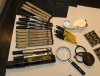
(...with the wooden chopsticks ! Or use something made of plastic .
Do not use metallic objects to stir an etching solution ! )
....

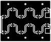
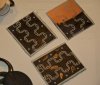
When etching is done ,remove the pcb ,and wash it with water ,thoroughly ,
so there will be no etching solution traces left on pcb ...


Notes :

-In cold etching solution ,procedure lasts long ,but results are really well etched pads/traces ...

-In warm (low heat ! ~40-50 °C) etching solution ,procedure really speeds up ,but marker cover ups may go off and
tracing is quite " rough "....
( ..Excess copper is removed under the toner print ...At the copper ~70-100um "profile " ...
Giving a "over-etched " apperance to traces/pads ...)

-Fresh Etching solution (transparent ) might cause deposition of copper on exposed aluminium of pcb .
(at sidecuts...Back of pcb ,still has the protective plastic film on ..) ..
Afterwards ,when etching is done,those copper deposits ,go -off easily by water ...
But under them ,aluminium is ..etched ..Tiny black holes ,where copper was ..Not deep ..
But if pcb is cut exactly in final size and there's no "head room " for some file work ....
Then ...It's pretty bad ....
So better to use some used ( bluish ) etching solution ,in that case ..
Etching solution ,that already contains some diluted copper (bluish color ) ,does not
affect aluminium ..
Then ,that phenomenon ,completely disappears ...

-Etching solution lasts long ...You do not throw it away ,after it's first use ..
You just add water and etching agent -when needed -,in same first solution..
It can be used for many etchings ...
(kept in a plastic bottle ..I.e of water ... ) .
When colour has become really blue ,then you'll have to find a way ,to properly , "throw it away " / dispose it ...
It's a toxic for the environment chemical ...
It contains really high amounts of metallic copper!
Meaning it kills almost every aquatic organism..
...You do not flush it in the sink !


-Stirring accelerates the process ...


...
 

Nutes and Nugs

Well-Known Member
I remember buying the PBC kits at RadioShack years ago.
Very good write up StarDust!!
Thanks, I just may be tempted to design and build one.
 

salmone

Well-Known Member
hi sds... hi guod... ups...hi all

...¿and the mcpcbs or star pcbs with cuore in Copper (Cu)?...

...maybe sinkpad SP-C40 COPPER ~0.040” (~1.0mm) SP-C60 COPPER ~0.059” (~1.50mm) to oslon or others leds...

check or follow...

http://www.candlepowerforums.com/vb/showthread.php?354907-Copper-mcpcb-comparison

http://www.led-tech.de/en/High-Power-LEDs-Cree/CREE-XM-Serie/CREE-XM-L-U2-on-Copper-PCB-LT-1790_120_170.html

or ceramic...

http://www.led-tech.de/en/High-Power-LEDs-Cree/CREE-XP-Series/CREE-XP-G-R5-on-Ceramic-PCB-LT-1713_120_138.html

...maybe sds or guod mcpcbs on copper cuore...or ceramic... ;-)

..sorry for the links...my intention is not to advertise brands ... only communicate ...
 

stardustsailor

Well-Known Member
. Double-sided exposure unit UV leds..
No ..I just use the laser printer/cloths iron technique ...
Way easier,less chemicals used ...
( Con: pcb with too thin traces (< 0.25 mm ) ,better to be done with UV tech )
 

salmone

Well-Known Member
thanks sds..

...maybe I need with some pcb's ...

...its not the best... but i think is doable...


...and yes there be wanting the other to the other side pcb.... but the idea is there...

saludos
 
Top