stardustsailor
Well-Known Member
In case you're using two high wattage (>80 Watt ) led drivers to power COB LED arrays or plenty of LEDs in series ,then spend a minute or two and read about this complete protection .
As for the actual circuit to be done ,all it takes is some average skills in soldering and nothin' much more than that .
The circuit to described below ,can be made in a perforated PCB prototyping board quite easily.
Even if you do not know shit about electronics and how those things actually work .....
https://www.google.gr/search?q=perforated pcb&tbm=isch&tbo=u&source=univ&sa=X&ved=0CB8QsARqFQoTCJ6o8aCwgccCFUntFAodvLQAFA&biw=1280&bih=891
(Thus the average soldering skills ...)
The finished board is made to protect LEDs and or COBs from fan failing and/ or from fan power supply failing .It also protects the timers that switch ON & OFF the drivers from accumulated inrush current ,
when two drivers are switched ON at the same time .That said ,the circuit will switch ON the first LED driver ,when it detects that the fan PSU is supplying with +12 VDC the fan and when the fan has reached more than ~350-400 rpm speed.
Then after few seconds it will switch ON the second LED driver.
If the fan ( or the fan PSU ) fails,both drivers will be switched OFF automatically ...
Once more ..Not much of electronics skills are needed to complete that circuit ...
A soldering iron ,some patience and of course the parts ....
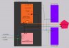
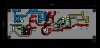
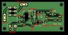
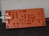
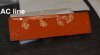
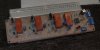
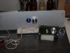
In the pic below is the board,bottom side view .
All the parts used are "through -hole " and of course are placed on the other side of the board.
Then the pins coming through the holes of the perforated pcb are soldered on the bottom side .
To connect parts-make the "trace" lines - , just use some thin and soft wiring
(plastic jacket isolated of course ,not bare copper=short circuits ).
It will look messy ,but who cares ,as long as it works ,providing safety and security ..
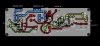
Some further explanations :
Red traces : +12 VDC Power Pathway
Yellow traces : TACH signal input from FAN ( 3 or 4 wire fan is needed )
Blue traces : Caution : 110 or 220 AC voltage !!!
(cover solder points with plenty of nail-polish ,as an extra safety measure & use thick,good isolated wiring )
Lime green : triggering signal pathway.
White-small- lines:
Show where -in which holes the pins of the parts are soldered
Grey area holes :
All the holes in the grey area have to be soldered to the same hole marked "-" ,
There are two holes like that ( at "12VDC IN & AUX VDC IN/OUT ).
DO NOT CONNECT THE HOLES ON THE GREY AREA IN SERIES .
THAT IS CALLED A "GROUND LOOP" and ain't a good thing ...
Just use plenty of black colored wire pieces and connect them to the same point ,from where
the board is/will be powered from (..from the FAN +12 VDC PSU ).
Diodes ( D2-D4 ,except D1 ) :
Marked with the letter "D" .
A means anode & C means cathode.
On the actual part ,the cathode side is usually marked with a line .
Capacitors:
Some are polarised .The + and - pins are marked where they should be soldered .
On the actual parts ,electrolytics have their "- " pin marked ,solid tantalum caps have their " +" pin marked .
Resistors:
Not much to say here ...Just solder them in the holes .
Q1 & D1 parts:
Those are three pin parts in a physical shape called " TO-92" .
Small black plastic things ,with one side flat and the other curved .
Place them on top side with the flat side ,as shown in the pic .
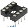
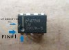
U1 part:
That is a small "chip" /Ic with 8 pins .(package : "DIP 8 "
As you look the actual part top-side pin #1 is the one at top-left (usually marked with a dot ,nearby).
At the pic the hole for pin #1 has a rectangular shape .All the other holes are oval.
Parts LIst :
R1 : 4700 OHMS (4K7)
R2 : 33'000 OHMS (33K )
R3 : 200'000 OHMS (200K ) - 1% TOLERANCE
*R4 : 470 OR 510 OHMS
R5 ,R6 : 5100 OHMS (5K1) - 1% TOLERANCE
R7,R8 : 510'000 OHMS (510K)
R9 : 2400 OHM (2K4)
R10 : 100 OHM
C1 : 10 - 47 uF ELECTROLYTIC OR SOLID TANTALUM , 25-35 V
C2 : 1 - 4,7 nF MKT OR POLYESTER
C3 : 47 -100 uF ELECTROLYTIC ,25-50 V
C4 : 1 - 2,2 uF ELECTROLYTIC OR SOLID TANTALUM ,25-35 V
C5,C6 : 100 nF MKT ,POLYESTER
(OR SOLID TANTALUM 25-35 V, " + " PINS TOWARDS GREEN TRACE LINE )
C7 : 1 uF ELECTROLYTIC OR SOLID TANTALUM ,25-35 V
D1 : 2N5064 SILICON CONTROLLED RECTIFIER (THYRISTOR )
D2,D3,D4 : 1N4148 SIGNAL DIODES
Q1 : 2N3904 NPN TRANSISTOR
U1 : LM 2917N-8 FREQUENCY TO VOLTAGE CONVERTER
* ALSO LM2907N-8 CAN BE USED ALTERNATIVELY ,BUT THEN R4 IS NOT NEEDED.
K1,K2 : DPDT (DOUBLE POLE-DOUBLE THROW ) 12VDC TRIGGER RELAYS, 250 VAC 8-10 A
Parts PDFs:
https://www.sparkfun.com/datasheets/Components/2N3904.pdf
http://www.ret.hu/DataSheets/28_TIRISZTOR/PHIS_007/2N5064.pdf
http://www.ti.com/lit/ds/symlink/lm2907-n.pdf
http://www.vishay.com/docs/81857/1n4148.pdf
http://www.farnell.com/datasheets/1360846.pdf
Good luck and all the best ,to the brave ones !
I'm pretty sure that you will be more than satisfied with the outcome!
Cheers.

As for the actual circuit to be done ,all it takes is some average skills in soldering and nothin' much more than that .
The circuit to described below ,can be made in a perforated PCB prototyping board quite easily.
Even if you do not know shit about electronics and how those things actually work .....
https://www.google.gr/search?q=perforated pcb&tbm=isch&tbo=u&source=univ&sa=X&ved=0CB8QsARqFQoTCJ6o8aCwgccCFUntFAodvLQAFA&biw=1280&bih=891
(Thus the average soldering skills ...)
The finished board is made to protect LEDs and or COBs from fan failing and/ or from fan power supply failing .It also protects the timers that switch ON & OFF the drivers from accumulated inrush current ,
when two drivers are switched ON at the same time .That said ,the circuit will switch ON the first LED driver ,when it detects that the fan PSU is supplying with +12 VDC the fan and when the fan has reached more than ~350-400 rpm speed.
Then after few seconds it will switch ON the second LED driver.
If the fan ( or the fan PSU ) fails,both drivers will be switched OFF automatically ...
Once more ..Not much of electronics skills are needed to complete that circuit ...
A soldering iron ,some patience and of course the parts ....
In the pic below is the board,bottom side view .
All the parts used are "through -hole " and of course are placed on the other side of the board.
Then the pins coming through the holes of the perforated pcb are soldered on the bottom side .
To connect parts-make the "trace" lines - , just use some thin and soft wiring
(plastic jacket isolated of course ,not bare copper=short circuits ).
It will look messy ,but who cares ,as long as it works ,providing safety and security ..
Some further explanations :
Red traces : +12 VDC Power Pathway
Yellow traces : TACH signal input from FAN ( 3 or 4 wire fan is needed )
Blue traces : Caution : 110 or 220 AC voltage !!!
(cover solder points with plenty of nail-polish ,as an extra safety measure & use thick,good isolated wiring )
Lime green : triggering signal pathway.
White-small- lines:
Show where -in which holes the pins of the parts are soldered
Grey area holes :
All the holes in the grey area have to be soldered to the same hole marked "-" ,
There are two holes like that ( at "12VDC IN & AUX VDC IN/OUT ).
DO NOT CONNECT THE HOLES ON THE GREY AREA IN SERIES .
THAT IS CALLED A "GROUND LOOP" and ain't a good thing ...
Just use plenty of black colored wire pieces and connect them to the same point ,from where
the board is/will be powered from (..from the FAN +12 VDC PSU ).
Diodes ( D2-D4 ,except D1 ) :
Marked with the letter "D" .
A means anode & C means cathode.
On the actual part ,the cathode side is usually marked with a line .
Capacitors:
Some are polarised .The + and - pins are marked where they should be soldered .
On the actual parts ,electrolytics have their "- " pin marked ,solid tantalum caps have their " +" pin marked .
Resistors:
Not much to say here ...Just solder them in the holes .
Q1 & D1 parts:
Those are three pin parts in a physical shape called " TO-92" .
Small black plastic things ,with one side flat and the other curved .
Place them on top side with the flat side ,as shown in the pic .
U1 part:
That is a small "chip" /Ic with 8 pins .(package : "DIP 8 "
As you look the actual part top-side pin #1 is the one at top-left (usually marked with a dot ,nearby).
At the pic the hole for pin #1 has a rectangular shape .All the other holes are oval.
Parts LIst :
R1 : 4700 OHMS (4K7)
R2 : 33'000 OHMS (33K )
R3 : 200'000 OHMS (200K ) - 1% TOLERANCE
*R4 : 470 OR 510 OHMS
R5 ,R6 : 5100 OHMS (5K1) - 1% TOLERANCE
R7,R8 : 510'000 OHMS (510K)
R9 : 2400 OHM (2K4)
R10 : 100 OHM
C1 : 10 - 47 uF ELECTROLYTIC OR SOLID TANTALUM , 25-35 V
C2 : 1 - 4,7 nF MKT OR POLYESTER
C3 : 47 -100 uF ELECTROLYTIC ,25-50 V
C4 : 1 - 2,2 uF ELECTROLYTIC OR SOLID TANTALUM ,25-35 V
C5,C6 : 100 nF MKT ,POLYESTER
(OR SOLID TANTALUM 25-35 V, " + " PINS TOWARDS GREEN TRACE LINE )
C7 : 1 uF ELECTROLYTIC OR SOLID TANTALUM ,25-35 V
D1 : 2N5064 SILICON CONTROLLED RECTIFIER (THYRISTOR )
D2,D3,D4 : 1N4148 SIGNAL DIODES
Q1 : 2N3904 NPN TRANSISTOR
U1 : LM 2917N-8 FREQUENCY TO VOLTAGE CONVERTER
* ALSO LM2907N-8 CAN BE USED ALTERNATIVELY ,BUT THEN R4 IS NOT NEEDED.
K1,K2 : DPDT (DOUBLE POLE-DOUBLE THROW ) 12VDC TRIGGER RELAYS, 250 VAC 8-10 A
Parts PDFs:
https://www.sparkfun.com/datasheets/Components/2N3904.pdf
http://www.ret.hu/DataSheets/28_TIRISZTOR/PHIS_007/2N5064.pdf
http://www.ti.com/lit/ds/symlink/lm2907-n.pdf
http://www.vishay.com/docs/81857/1n4148.pdf
http://www.farnell.com/datasheets/1360846.pdf
Good luck and all the best ,to the brave ones !
I'm pretty sure that you will be more than satisfied with the outcome!
Cheers.
Last edited: