stardustsailor
Well-Known Member
- Epoxy doesn't stick to Anodised Aluminium .
-Almost all alloys of soft alum ( 5xxxx 6xxxx 1xxxx ) they form a protective- to further corrosion -,superficial layer of Alum .oxide ..
Alumina .Which is transparent .
And while soft alum is way heat conductive,alumina has ~10x less thermal conductivity values ...
Alumina is the main reason that aluminium cannot be painted or adhere with glue ,easy ....
-To overcome this problem ,brushing the alum with hard Scotchbrite sponge can remove Alumina
or using a fine ( ~100-200 ) sandpaper is another way ...
But alum reacts with oxygen of air ,and alumina is forming rapidly again ....
-Epoxy will stick ,but eventually it will peel off (as a thin film of ~ 0.1mm ),after a certain period of time ...
-So "passivation" of alum surface is needed ...
Aluminium etch primers ....
Toxic and dangerous.
(Alodine ,ect...Usually part A/first step =defatting sovent +Phosphoric Acid Part B /second step = Chromic +6 acid )
And epoxy has to be applied really soon after the surface priming procedures ....
http://www.jamestowndistributors.com/userportal/show_product.do?pid=12214
But it will adhere ,once and for all ....
.........................................................................................................................................................
Now .....
Turn the epoxy ,into thermal conductive ,dielectric bonding agent...
Tricky .....
Best market-available epoxies have 0.8 to 3 W/m.K :
Bergquist : 1.1 -2.2 W/m.K
Laird : 2-3 W/m.K
DuPont : 0.8 W/m.K
Fischer Electronik : 0.8 W/m.K
Iteq : 2.2 W/m.K
Taconic : 2 W/m.K
ResinLab : 1-2 W/m.K
Make your own ....
-thermal epoxy has to have the lowest viscosity possible .
(ensuring good wettability ,consistence,coverage and homogeneity -no air bubbles/pockets )
-Normal,low viscosity, liquid epoxy has to be mixed with dielectric ,thermal conductive filler .
Filler load should be low to moderate ( 5-20% of volume ),otherwise the epoxy will become thick (putty..)
Smallest particle Dia of ceramic is desirable ...
Two main ceramics here ..
BeO ( Beryllium Oxide ) with highest thermal conductivity ,after diamond ,
but way toxic ...
https://en.wikipedia.org/wiki/Beryllium_oxide
https://en.wikipedia.org/wiki/List_of_thermal_conductivities
BN ( Boron Nitride )
https://en.wikipedia.org/wiki/Boron_nitride
http://www.asburystore.com/ProductDetails.asp?ProductCode=BN5800-1LB
....................................................................................................................................
-Now ...After those .....
Epoxy will be dielectric and thermally conductive ,while it will adhere to alum surface of heatsink ....
What remains to be solved is the exact procedure of "sandwiching " heatsink -epoxy(dielectric layer ) and copper foil ....
Epoxy should be applied in one-phase or two phase procedure ?
If one phase ,the epoxy has to be applied in relatively thick layer and more "dense" (more BN load ) ,evenly and carefully ,
to the freshly primed heatsink and the copper foil should be layered on top ,and all together , be put inside the hot-press for curing ..
(or clamped and onto the oven ) ...
Thickness of epoxy should be no more of 0.1 mm (100 um ) ..
Heatsink and copper foil should not contact at all ...
If "two phase ",one first layer of epoxy ( ~50 um ) is applied and let to fully cure (harden ).
Then copper foil is layered on top ,with another ~50 um layer of epoxy ...
Again pressed together and let cure in elevated temps ( see epoxy manual for that .. )
....
Then on to copper etching ..
Carefull there also ...
-Iron (III ) Chloride ,should not come in contact with rest of aluminium heatsink ,except copper(& epoxy underneath ) surface ..
-Almost all alloys of soft alum ( 5xxxx 6xxxx 1xxxx ) they form a protective- to further corrosion -,superficial layer of Alum .oxide ..
Alumina .Which is transparent .
And while soft alum is way heat conductive,alumina has ~10x less thermal conductivity values ...
Alumina is the main reason that aluminium cannot be painted or adhere with glue ,easy ....
-To overcome this problem ,brushing the alum with hard Scotchbrite sponge can remove Alumina
or using a fine ( ~100-200 ) sandpaper is another way ...
But alum reacts with oxygen of air ,and alumina is forming rapidly again ....
-Epoxy will stick ,but eventually it will peel off (as a thin film of ~ 0.1mm ),after a certain period of time ...
-So "passivation" of alum surface is needed ...
Aluminium etch primers ....
Toxic and dangerous.
(Alodine ,ect...Usually part A/first step =defatting sovent +Phosphoric Acid Part B /second step = Chromic +6 acid )
And epoxy has to be applied really soon after the surface priming procedures ....
http://www.jamestowndistributors.com/userportal/show_product.do?pid=12214
But it will adhere ,once and for all ....
.........................................................................................................................................................
Now .....
Turn the epoxy ,into thermal conductive ,dielectric bonding agent...
Tricky .....
-Thermal conductivity of epoxy should rise from 0.2-0.5 W/m.K to > 0.8 W/m.KCost Drivers For MCPCBs
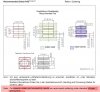
Dielectric Substrate
The # 1 cost component of the MCPCB is the dielectric substrate between the copper traces and the metal heatsink / core.
Definition
An insulating medium which occupies the region between two conductors. In this case, the copper circuits and the metal core heat sink.
https://heatsinks.files.wordpress.com/2011/02/mcpcbs-for-led-applications.pdf
Best market-available epoxies have 0.8 to 3 W/m.K :
Bergquist : 1.1 -2.2 W/m.K
Laird : 2-3 W/m.K
DuPont : 0.8 W/m.K
Fischer Electronik : 0.8 W/m.K
Iteq : 2.2 W/m.K
Taconic : 2 W/m.K
ResinLab : 1-2 W/m.K
Make your own ....
-thermal epoxy has to have the lowest viscosity possible .
(ensuring good wettability ,consistence,coverage and homogeneity -no air bubbles/pockets )
-Normal,low viscosity, liquid epoxy has to be mixed with dielectric ,thermal conductive filler .
Filler load should be low to moderate ( 5-20% of volume ),otherwise the epoxy will become thick (putty..)
Smallest particle Dia of ceramic is desirable ...
Two main ceramics here ..
BeO ( Beryllium Oxide ) with highest thermal conductivity ,after diamond ,
but way toxic ...
https://en.wikipedia.org/wiki/Beryllium_oxide
https://en.wikipedia.org/wiki/List_of_thermal_conductivities
BN ( Boron Nitride )
https://en.wikipedia.org/wiki/Boron_nitride
http://www.asburystore.com/ProductDetails.asp?ProductCode=BN5800-1LB
....................................................................................................................................
-Now ...After those .....
Epoxy will be dielectric and thermally conductive ,while it will adhere to alum surface of heatsink ....
What remains to be solved is the exact procedure of "sandwiching " heatsink -epoxy(dielectric layer ) and copper foil ....
Epoxy should be applied in one-phase or two phase procedure ?
If one phase ,the epoxy has to be applied in relatively thick layer and more "dense" (more BN load ) ,evenly and carefully ,
to the freshly primed heatsink and the copper foil should be layered on top ,and all together , be put inside the hot-press for curing ..
(or clamped and onto the oven ) ...
Thickness of epoxy should be no more of 0.1 mm (100 um ) ..
Heatsink and copper foil should not contact at all ...
If "two phase ",one first layer of epoxy ( ~50 um ) is applied and let to fully cure (harden ).
Then copper foil is layered on top ,with another ~50 um layer of epoxy ...
Again pressed together and let cure in elevated temps ( see epoxy manual for that .. )
....
Then on to copper etching ..
Carefull there also ...
-Iron (III ) Chloride ,should not come in contact with rest of aluminium heatsink ,except copper(& epoxy underneath ) surface ..
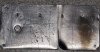
 oor Resistance .Almost peels off .