Light-emitting diode
Light-emitting diode

Red, pure green and blue LEDs of the 5mm diffused typeType
Passive,
optoelectronicWorking principle
ElectroluminescenceInvented
Nick Holonyak Jr. (1962)
Electronic symbol

Pin configuration
anode and
cathode


Parts of an LED. Although not directly labeled, the flat bottom surfaces of the anvil and post embedded inside the epoxy act as anchors, to prevent the conductors from being forcefully pulled out from mechanical strain or vibration.

LED spotlight using 38 individual diodes for powering from
mains voltage

Dual-wavelength LED in
SMD housing
A
light-emitting diode (
LED) is a
semiconductor light source.
[1] LEDs are used as indicator lamps in many devices and are increasingly used for other
lighting. Introduced as a practical electronic component in 1962,
[2] early LEDs emitted low-intensity red light, but modern versions are available across the
visible,
ultraviolet and
infrared wavelengths, with very high brightness.
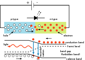
When a light-emitting
diode is forward
biased (switched on),
electrons are able to
recombine with
electron holes within the device, releasing energy in the form of
photons. This effect is called
electroluminescence and the
color of the light (corresponding to the energy of the photon) is determined by the
energy gap of the semiconductor. LEDs are often small in area (less than 1 mm
2), and integrated optical components may be used to shape its radiation pattern.
[3] LEDs present many
advantages over incandescent light sources including
lower energy consumption, longer
lifetime, improved robustness, smaller size, faster switching, and greater durability and reliability. LEDs powerful enough for room lighting are relatively expensive and require more precise current and
heat management than compact
fluorescent lamp sources of comparable output.
Light-emitting diodes are used in applications as diverse as replacements for
aviation lighting,
automotive lighting (particularly brake lamps, turn signals and
indicators) as well as in
traffic signals. The advantages of LEDs mentioned above have allowed new text and video displays and sensors to be developed, while their high switching rates are also useful in advanced communications technology.
Infrared LEDs are also used in the
remote control units of many commercial products including televisions, DVD players, and other domestic appliances.

Green electroluminescence from a point contact on a crystal of
SiC recreates
H. J. Round's original experiment from 1907.
Electroluminescence as a phenomenon was discovered in 1907 by the British experimenter
H. J. Round of
Marconi Labs, using a crystal of
silicon carbide and a
cat's-whisker detector.
[4][5] Russian
Oleg Vladimirovich Losev reported on the creation of a first LED in 1927.
[6][7] His research was distributed in Russian, German and British scientific journals, but no practical use was made of the discovery for several decades.
[8][9] Rubin Braunstein of the
Radio Corporation of America reported on infrared emission from
gallium arsenide (GaAs) and other semiconductor alloys in 1955.
[10] Braunstein observed infrared emission generated by simple diode structures using
gallium antimonide (GaSb), GaAs,
indium phosphide (InP), and
silicon-germanium (SiGe) alloys at room temperature and at 77 kelvin.
In 1961, American experimenters Robert Biard and Gary Pittman working at
Texas Instruments,
[11] found that GaAs emitted infrared radiation when electric current was applied and received the patent for the infrared LED.
The first practical visible-spectrum (red) LED was developed in 1962 by
Nick Holonyak Jr., while working at
General Electric Company.
[2] Holonyak is seen as the "father of the light-emitting diode".
[12] M. George Craford,
[13] a former graduate student of Holonyak, invented the first yellow LED and improved the brightness of red and red-orange LEDs by a factor of ten in 1972.
[14] In 1976, T.P. Pearsall created the first high-brightness, high efficiency LEDs for optical fiber telecommunications by inventing new semiconductor materials specifically adapted to optical fiber transmission wavelengths.
[15]
Until 1968, visible and infrared LEDs were extremely costly, on the order of US $200 per unit, and so had little practical use.
[16] The
Monsanto Company was the first organization to mass-produce visible LEDs, using gallium arsenide phosphide in 1968 to produce red LEDs suitable for indicators.
[16] Hewlett Packard (HP) introduced LEDs in 1968, initially using GaAsP supplied by Monsanto. The technology proved to have major uses for alphanumeric displays and was integrated into HP's early handheld calculators. In the 1970s commercially successful LED devices at under five cents each were produced by Fairchild Optoelectronics. These devices employed compound semiconductor chips fabricated with the
planar process invented by Dr. Jean Hoerni at
Fairchild Semiconductor.
[17] The combination of planar processing for chip fabrication and innovative packaging methods enabled the team at Fairchild led by optoelectronics pioneer Thomas Brandt to achieve the needed cost reductions. These methods continue to be used by LED producers.
The first commercial LEDs were commonly used as replacements for
incandescent and
neon indicator lamps, and in
seven-segment displays,
[19] first in expensive equipment such as laboratory and electronics test equipment, then later in such appliances as TVs, radios, telephones, calculators, and even watches (see list of
signal uses). These red LEDs were bright enough only for use as indicators, as the light output was not enough to illuminate an area. Readouts in calculators were so small that plastic lenses were built over each digit to make them legible. Later, other colors grew widely available and also appeared in appliances and equipment. As LED materials technology grew more advanced, light output rose, while maintaining efficiency and reliability at acceptable levels. The invention and development of the high power white light LED led to use for illumination, which is fast replacing incandescent and fluorescent lighting.
[20][21] (see list of
illumination applications). Most LEDs were made in the very common 5 mm T1¾ and 3 mm T1 packages, but with rising power output, it has grown increasingly necessary to shed excess heat to maintain reliability,
[22] so more complex packages have been adapted for efficient heat dissipation. Packages for state-of-the-art
high power LEDs bear little resemblance to early LEDs.

Illustration of
Haitz's Law. Light output per LED as a function of production year, note the logarithmic scale on the vertical axis.
Continuing development
The first high-brightness blue LED was demonstrated by
Shuji Nakamura of
Nichia Corporation and was based on
InGaN borrowing on critical developments in
GaN nucleation on sapphire substrates and the demonstration of p-type doping of GaN which were developed by
Isamu Akasaki and H. Amano in
Nagoya. In 1995,
Alberto Barbieri at the
Cardiff University Laboratory (GB) investigated the efficiency and reliability of high-brightness LEDs and demonstrated a very impressive result by using a transparent contact made of
indium tin oxide (ITO) on (AlGaInP/GaAs) LED. The existence of blue LEDs and high efficiency LEDs quickly led to the development of the first
white LED, which employed a Y
3Al
5O
12:Ce, or "
YAG", phosphor coating to mix yellow (down-converted) light with blue to produce light that appears white. Nakamura was awarded the 2006
Millennium Technology Prize for his invention.
[23]
The development of LED technology has caused their efficiency and light output to
rise exponentially, with a doubling occurring about every 36 months since the 1960s, in a way similar to
Moore's law. The advances are generally attributed to the parallel development of other semiconductor technologies and advances in optics and material science. This trend is normally called
Haitz's Law after Dr. Roland Haitz.
In February 2008, 300
lumens of visible light per watt
luminous efficacy (not per electrical watt) and warm-light emission was achieved by using
nanocrystals.
[25]
In 2009, a process for growing gallium nitride (GaN) LEDs on silicon has been reported.
Epitaxy costs could be reduced by up to 90% using six-inch silicon wafers instead of two-inch sapphire wafers.
Technology
The inner workings of an LED
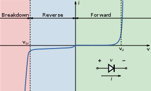
I-V diagram for a
diode. An LED will begin to emit light when the on-
voltage is exceeded. Typical on voltages are 23
volts
Physics
The LED consists of a chip of semiconducting material
doped with impurities to create a
p-n junction. As in other diodes, current flows easily from the p-side, or
anode, to the n-side, or
cathode, but not in the reverse direction. Charge-carriers
electrons and
holesflow into the junction from
electrodes with different voltages. When an electron meets a hole, it falls into a lower
energy level, and releases
energy in the form of a
photon.
The
wavelength of the light emitted, and thus its color depends on the
band gap energy of the materials forming the
p-n junction. In
silicon or
germanium diodes, the electrons and holes recombine by a
non-radiative transition which produces no optical emission, because these are
indirect band gap materials. The materials used for the LED have a
direct band gap with energies corresponding to near-infrared, visible or near-ultraviolet light.
LED development began with infrared and red devices made with
gallium arsenide. Advances in
materials science have enabled making devices with ever-shorter wavelengths, emitting light in a variety of colors.
LEDs are usually built on an n-type substrate, with an electrode attached to the p-type layer deposited on its surface. P-type substrates, while less common, occur as well. Many commercial LEDs, especially GaN/InGaN, also use
sapphire substrate.
Most materials used for LED production have very high
refractive indices. This means that much light will be reflected back into the material at the material/air surface interface. Thus,
light extraction in LEDs is an important aspect of LED production, subject to much research and development.
Refractive index

Idealized example of light emission cones in a semiconductor, for a single point-source emission zone. The left illustration is for a fully translucent wafer, while the right illustration shows the half-cones formed when the bottom layer is fully opaque. The light is actually emitted equally in all directions from the point-source, so the areas between the cones shows the large amount of trapped light energy that is wasted as heat.
[27]
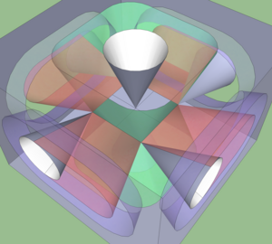
The light emission cones of a real LED wafer are far more complex than a single point-source light emission. Typically the light emission zone is a 2D plane between the wafers. Across this 2D plane, there is effectively a separate set of emission cones for every atom.
Drawing the billions of overlapping cones is impossible, so this is a simplified diagram showing the extents of all the emission cones combined. The larger side cones are clipped to show the interior features and reduce image complexity; they would extend to the opposite edges of the 2D emission plane.
Bare uncoated semiconductors such as
silicon exhibit a very high
refractive index relative to open air, which prevents passage of photons at sharp angles relative to the air-contacting surface of the semiconductor. This property affects both the light-emission efficiency of LEDs as well as the light-absorption efficiency of
photovoltaic cells. The refractive index of silicon is 4.24, while air is 1.00002926
[28]
Generally a flat-surfaced uncoated LED semiconductor chip will only emit light perpendicular to the semiconductor's surface, and a few degrees to the side, in a cone shape referred to as the
light cone,
cone of light,
[29] or the
escape cone.
[27] The maximum
angle of incidence is referred to as the
critical angle. When this angle is exceeded photons no longer penetrate the semiconductor, but are instead reflected both internally inside the semiconductor crystal, and externally off the surface of the crystal as if it were a
mirror.
[27]
Internal reflections can escape through other crystalline faces, if the incidence angle is low enough and the crystal is sufficiently transparent to not re-absorb the photon emission. But for a simple square LED with 90-degree angled surfaces on all sides, the faces all act as equal angle mirrors. In this case the light can not escape and is lost as waste heat in the crystal.
[27]
A convoluted chip surface with angled
facets similar to a jewel or
fresnel lens can increase light output by allowing light to be emitted perpendicular to the chip surface while far to the sides of the photon emission point.
[30]
The ideal shape of a semiconductor with maximum light output would be a
microsphere with the photon emission occurring at the exact center, with electrodes penetrating to the center to contact at the emission point. All light rays emanating from the center would be perpendicular to the entire surface of the sphere, resulting in no internal reflections. A hemispherical semiconductor would also work, with the flat back-surface serving as a mirror to back-scattered photons.
[31]
Transition coatings
Many LED semiconductor chips are
potted in clear or colored molded plastic shells. The plastic shell has three purposes:
- Mounting the semiconductor chip in devices is easier to accomplish.
- The tiny fragile electrical wiring is physically supported and protected from damage
- The plastic acts as a refractive intermediary between the relatively high-index semiconductor and low-index open air.[32]
The third feature helps to boost the light emission from the semiconductor by acting as a diffusing lens, allowing light to be emitted at a much higher angle of incidence from the light cone, than the bare chip is able to emit alone.
Efficiency and operational parameters
Typical indicator LEDs are designed to operate with no more than 3060
mW of electrical power. Around 1999,
Philips Lumileds introduced power LEDs capable of continuous use at one
watt. These LEDs used much larger semiconductor die sizes to handle the large power inputs. Also, the semiconductor dies were mounted onto metal slugs to allow for heat removal from the LED die.
One of the key advantages of LED-based lighting sources is high
luminous efficacy. White LEDs quickly matched and overtook the efficacy of standard incandescent lighting systems. In 2002, Lumileds made five-watt LEDs available with a
luminous efficacy of 1822 lumens per watt (lm/W). For comparison, a conventional 60100 W
incandescent light bulb emits around 15 lm/W, and standard
fluorescent lights emit up to 100 lm/W. A recurring problem is that efficacy falls sharply with rising current. This effect is known as
droop and effectively limits the light output of a given LED, raising heating more than light output for higher current.
[33][34]
In September 2003, a new type of blue LED was demonstrated by the company
Cree Inc. to provide 24 mW at 20
milliamperes (mA). This produced a commercially packaged white light giving 65 lm/W at 20 mA, becoming the brightest white LED commercially available at the time, and more than four times as efficient as standard incandescents. In 2006, they demonstrated a prototype with a record white LED luminous efficacy of 131 lm/W at 20 mA.
Nichia Corporation has developed a white LED with luminous efficacy of 150 lm/W at a forward current of 20 mA.
[36] Cree's XLamp XM-L LEDs, commercially available in 2011, produce 100 lumens per watt at their full power of 10 watts, and up to 160 lumens/watt at around 2 watts input power.
Practical general lighting needs high-power LEDs, of one watt or more. Typical operating currents for such devices begin at 350 mA.
Note that these efficiencies are for the LED chip only, held at low temperature in a lab. Lighting works at higher temperature and with drive circuit losses, so efficiencies are much lower.
United States Department of Energy (DOE) testing of commercial LED lamps designed to replace incandescent lamps or
CFLs showed that average efficacy was still about 46 lm/W in 2009 (tested performance ranged from 17 lm/W to 79 lm/W).
[37]
Cree issued a press release on February 3, 2010 about a laboratory prototype LED achieving 208 lumens per watt at room temperature. The correlated
color temperature was reported to be 4579 K.
Lifetime and failure
Main article:
List of LED failure modes
Solid state devices such as LEDs are subject to very limited
wear and tear if operated at low currents and at low temperatures. Many of the LEDs made in the 1970s and 1980s are still in service today. Typical lifetimes quoted are 25,000 to 100,000 hours but heat and current settings can extend or shorten this time significantly.
[39]
The most common symptom of LED (and
diode laser) failure is the gradual lowering of light output and loss of efficiency. Sudden failures, although rare, can occur as well. Early red LEDs were notable for their short lifetime. With the development of high-power LEDs the devices are subjected to higher
junction temperatures and higher current densities than traditional devices. This causes stress on the material and may cause early light-output degradation. To quantitatively classify lifetime in a standardized manner it has been suggested to use the terms L75 and L50 which is the time it will take a given LED to reach 75% and 50% light output respectively.
[40]
Like other lighting devices, LED performance is temperature dependent. Most manufacturers published ratings of LEDs are for an operating temperature of 25 °C. LEDs used outdoors, such as traffic signals or in-pavement signal lights, and that are utilized in climates where the temperature within the luminaire gets very hot, could result in low signal intensities or even failure.
[41]
LED light output actually rises at colder temperatures (leveling off depending on type at around −30C
[citation needed]). Consequently, LED technology may be a good replacement in uses such as supermarket freezer lighting
[42][43][44] and will last longer than other technologies. Because LEDs emit less heat than incandescent bulbs, they are an energy-efficient technology for uses such as freezers. However, because they emit little heat, ice and snow may build up on the LED luminaire in colder climates.
[41] This lack of waste heat generation has been observed to cause sometimes significant problems with street traffic signals and airport runway lighting in snow-prone areas, although some research has been done to try to develop heat sink technologies to transfer heat to other areas of the luminaire.
Colors and materials
Conventional LEDs are made from a variety of inorganic
semiconductor materials, the following table shows the available colors with wavelength range, voltage drop and material:
Color
Wavelength [nm]Voltage [V]Semiconductor material
Infraredλ > 760
ΔV < 1.9
Gallium arsenide (GaAs)
Aluminium gallium arsenide (AlGaAs)
Red610 <
λ < 7601.63 < Δ
V < 2.03
Aluminium gallium arsenide (AlGaAs)
Gallium arsenide phosphide (GaAsP)
Aluminium gallium indium phosphide (AlGaInP)
Gallium(III) phosphide (GaP)
Orange590 <
λ < 6102.03 < Δ
V < 2.10
Gallium arsenide phosphide (GaAsP)
Aluminium gallium indium phosphide (AlGaInP)
Gallium(III) phosphide (GaP)
Yellow570 <
λ < 5902.10 < Δ
V < 2.18
Gallium arsenide phosphide (GaAsP)
Aluminium gallium indium phosphide (AlGaInP)
Gallium(III) phosphide (GaP)
Green500 <
λ < 5701.9
[46] < Δ
V < 4.0
Indium gallium nitride (InGaN) /
Gallium(III) nitride (GaN)
Gallium(III) phosphide (GaP)
Aluminium gallium indium phosphide (AlGaInP)
Aluminium gallium phosphide (AlGaP)
Blue450 <
λ < 5002.48 < Δ
V < 3.7
Zinc selenide (ZnSe)
Indium gallium nitride (InGaN)
Silicon carbide (SiC) as substrate
Silicon (Si) as substrate (under development)
Violet400 <
λ < 4502.76 < Δ
V < 4.0
Indium gallium nitride (InGaN)
Purplemultiple types2.48 < Δ
V < 3.7Dual blue/red LEDs,
blue with red phosphor,
or white with purple plastic
Ultravioletλ < 4003.1 < Δ
V < 4.4
Diamond (235 nm)
[47]
Boron nitride (215 nm)
[48][49]
Aluminium nitride (AlN) (210 nm)
[50]
Aluminium gallium nitride (AlGaN)
Aluminium gallium indium nitride (AlGaInN) (down to 210 nm)
[51]WhiteBroad spectrumΔ
V = 3.5Blue/UV diode with yellow phosphor
[edit] Ultraviolet and
blue LEDs
 Blue
Blue LEDs.
Current bright blue LEDs are based on the wide
band gap semiconductors GaN (
gallium nitride) and
InGaN (indium gallium nitride). They can be added to existing red and green LEDs to produce the impression of white light, though white LEDs today rarely use this principle.
The first blue LEDs using gallium nitride were made in 1971 by Jacques Pankove at
RCA Laboratories.
[52] These devices had too little light output to be of practical use and research into gallium nitride devices slowed. In August 1989, Cree Inc. introduced the first commercially available blue LED based on the
indirect bandgap semiconductor, silicon carbide.
[53] SiC LEDs had very low effiency, no more than about 0.03%, but did emit in the blue portion of the visible light spectrum.
In the late 1980s, key breakthroughs in GaN
epitaxial growth and
p-type doping
[54] ushered in the modern era of GaN-based optoelectronic devices. Building upon this foundation, in 1993 high brightness blue LEDs were demonstrated. Efficiency (light energy produced vs. electrical energy used) reached 10%.
[55] High-brightness blue LEDs invented by
Shuji Nakamura of
Nichia Corporation using gallium nitride revolutionized LED lighting, making high-power light sources practical.
By the late 1990s, blue LEDs had become widely available. They have an active region consisting of one or more InGaN
quantum wells sandwiched between thicker layers of GaN, called cladding layers. By varying the relative InN-GaN fraction in the InGaN quantum wells, the light emission can be varied from violet to amber. AlGaN
aluminium gallium nitride of varying AlN fraction can be used to manufacture the cladding and quantum well layers for ultraviolet LEDs, but these devices have not yet reached the level of efficiency and technological maturity of the InGaN-GaN blue/green devices. If the active quantum well layers are GaN, instead of alloyed InGaN or AlGaN, the device will emit near-ultraviolet light with wavelengths around 350370 nm. Green LEDs manufactured from the InGaN-GaN system are far more efficient and brighter than green LEDs produced with non-nitride material systems.
With nitrides containing aluminium, most often
AlGaN and
AlGaInN, even shorter wavelengths are achievable. Ultraviolet LEDs in a range of wavelengths are becoming available on the market. Near-UV emitters at wavelengths around 375395 nm are already cheap and often encountered, for example, as
black light lamp replacements for inspection of anti-
counterfeiting UV watermarks in some documents and paper currencies. Shorter wavelength diodes, while substantially more expensive, are commercially available for wavelengths down to 247 nm.
[56] As the photosensitivity of microorganisms approximately matches the absorption spectrum of
DNA, with a peak at about 260 nm, UV LED emitting at 250270 nm are to be expected in prospective disinfection and sterilization devices. Recent research has shown that commercially available UVA LEDs (365 nm) are already effective disinfection and sterilization devices.
[57]
Deep-UV wavelengths were obtained in laboratories using
aluminium nitride (210 nm),
[50] boron nitride (215 nm)
[48][49] and
diamond (235 nm).
[47]
White light
There are two primary ways of producing high intensity white-light using LEDs. One is to use individual LEDs that emit three
primary colors[58]red, green, and blueand then mix all the colors to form white light. The other is to use a phosphor material to convert monochromatic light from a blue or UV LED to broad-spectrum white light, much in the same way a fluorescent light bulb works.
Due to
metamerism, it is possible to have quite different spectra that appear white.
RGB systems

Combined spectral curves for blue, yellow-green, and high brightness red solid-state semiconductor LEDs.
FWHM spectral bandwidth is approximately 2427 nm for all three colors.
White light can be formed by mixing differently colored lights; the most common method is to use
red, green and blue (RGB). Hence the method is called multi-colored white LEDs (sometimes referred to as Red Green Blue LEDs). Because these need electronic circuits to control the blending and
diffusion of different colors, these are seldom used to produce white lighting. Nevertheless, this method is particularly interesting in many uses because of the flexibility of mixing different colors,
[59] and, in principle, this mechanism also has higher quantum efficiency in producing white light.
There are several types of multi-colored white LEDs:
di-,
tri-, and
tetrachromatic white LEDs. Several key factors that play among these different methods, include color stability,
color rendering capability, and
luminous efficacy. Often higher efficiency will mean lower color rendering, presenting a trade off between the luminous efficiency and color rendering. For example, the dichromatic white LEDs have the best luminous efficacy (120 lm/W), but the lowest color rendering capability. Conversely, although
tetrachromatic white LEDs have excellent color rendering capability, they often have poor luminous efficiency. Trichromatic white LEDs are in between, having both good luminous efficacy (>70 lm/W) and fair color rendering capability.
Multi-color LEDs offer not merely another means to form white light, but a new means to form light of different colors. Most
perceivable colors can be formed by mixing different amounts of three primary colors. This allows precise dynamic color control. As more effort is devoted to investigating this method, multi-color LEDs should have profound influence on the fundamental method which we use to produce and control light color. However, before this type of LED can play a role on the market, several technical problems need solving. These include that this type of LED's emission power
decays exponentially with rising temperature,
[60] resulting in a substantial change in color stability. Such problems inhibit and may preclude industrial use. Thus, many new package designs aimed at solving this problem have been proposed and their results are now being reproduced by researchers and scientists.
Phosphor-based LEDs
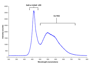
Spectrum of a white LED clearly showing blue light which is directly emitted by the GaN-based LED (peak at about 465 nm) and the more broadband
Stokes-shifted light emitted by the Ce3+:YAG phosphor which emits at roughly 500700 nm.
This method involves
coating an LED of one color (mostly blue LED made of InGaN) with
phosphor of different colors to form white light; the resultant LEDs are called
phosphor-based white LEDs.
[61] A fraction of the blue light undergoes the
Stokes shift being transformed from shorter wavelengths to longer. Depending on the color of the original LED, phosphors of different colors can be employed. If several phosphor layers of distinct colors are applied, the emitted spectrum is broadened, effectively raising the
color rendering index (CRI) value of a given LED.
[62]
Phosphor based LEDs have a lower efficiency than normal LEDs due to the heat loss from the Stokes shift and also other phosphor-related degradation issues. However, the phosphor method is still the most popular method for making
high intensity white LEDs. The design and production of a light source or light fixture using a monochrome emitter with phosphor conversion is simpler and cheaper than a complex
RGB system, and the majority of high intensity white LEDs presently on the market are manufactured using phosphor light conversion.
The greatest barrier to high efficiency is the seemingly unavoidable Stokes energy loss. However, much effort is being spent on optimizing these devices to higher light output and higher operation temperatures. For instance, the efficiency can be raised by adapting better package design or by using a more suitable type of phosphor. Philips Lumileds' patented conformal coating process addresses the issue of varying phosphor thickness, giving the white LEDs a more homogeneous white light.
[63] With development ongoing, the efficiency of phosphor based LEDs generally rises with each new product announcement.
The phosphor based white LEDs encapsulate InGaN blue LEDs inside phosphor coated epoxy. A common yellow phosphor material is
cerium-
doped yttrium aluminium garnet (Ce
3+:YAG).
White LEDs can also be made by
coating near
ultraviolet (NUV) emitting LEDs with a mixture of high efficiency
europium-based red and blue emitting phosphors plus green emitting copper and aluminium doped zinc sulfide (ZnS:Cu, Al). This is a method analogous to the way
fluorescent lamps work. This method is less efficient than the blue LED with YAG:Ce phosphor, as the
Stokes shift is larger, so more energy is converted to heat, but yields light with better spectral characteristics, which render color better. Due to the higher radiative output of the ultraviolet LEDs than of the blue ones, both methods offer comparable brightness. A concern is that UV light may leak from a malfunctioning light source and cause harm to human eyes or skin.
Other white LEDs
Another method used to produce experimental white light LEDs used no phosphors at all and was based on
homoepitaxially grown
zinc selenide (ZnSe) on a ZnSe substrate which simultaneously emitted blue light from its active region and yellow light from the substrate.
[64]
Organic light-emitting diodes (OLEDs)
Main article:
Organic light-emitting diode

Demonstration of a
flexible OLED device
In an organic light emitting diode (
OLED), the
electroluminescent material comprising the emissive layer of the diode is an
organic compound. The organic material is electrically conductive due to the
delocalization of pi electrons caused by
conjugation over all or part of the molecule, and the material therefore functions as an
organic semiconductor.
[65] The organic materials can be small organic
molecules in a
crystalline phase, or
polymers.
The potential advantages of OLEDs include thin, low cost displays with a low driving voltage, wide viewing angle and high contrast and color gamut.
[66] Polymer LEDs have the added benefit of printable
[67][68] and
flexible[69] displays. OLEDs have been used to make visual displays for portable electronic devices such as cellphones, digital cameras, and MP3 players while possible future uses include lighting and televisions.
[66]
Quantum dot LEDs (experimental)
Quantum dots (QD) are semiconductor
nanocrystals that possess unique optical properties.
[70] Their emission color can be tuned from the visible throughout the infrared spectrum. This allows quantum dot LEDs to create almost any color on the
CIE diagram. This provides more color options and better color rendering than white LEDs.
[citation needed] Quantum dot LEDs are available in the same package types as traditional
phosphor based LEDs.
[citation needed] One example of this is a method developed by Michael Bowers, at
Vanderbilt University in Nashville, involving coating a blue LED with
quantum dots that glow white in response to the blue light from the LED. This method emits a warm, yellowish-white light similar to that made by
incandescent bulbs.
[71] Quantum dots are also being considered for use in white light emitting diodes in liquid crystal display (LCD) televisions.
[72]
The major difficulty in using quantum dots based LEDs is the insufficient stability of QDs under prolonged irradiation.
[citation needed] In February 2011 scientists at PlasmaChem GmbH could synthesize quantum dots for LED applications and build a light converter on their basis, which could efficiently convert light from blue to any other color for many hundred hours.
[citation needed] Such QDs can be used to emit visible or near infrared light of any wavelength being excited by light with a shorter wavelength.
Types
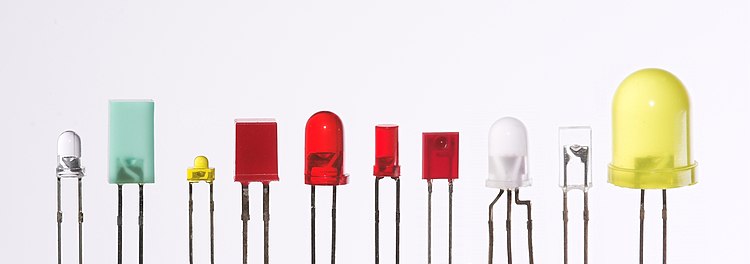
LEDs are produced in a variety of shapes and sizes. The 5 mm cylindrical package (red, fifth from the left) is the most common, estimated at 80% of world production.[
citation needed] The color of the plastic lens is often the same as the actual color of light emitted, but not always. For instance, purple plastic is often used for
infrared LEDs, and most blue devices have clear housings. There are also LEDs in
SMT packages, such as those found on
blinkies and on cell phone keypads (not shown).
The main types of LEDs are miniature, high power devices and custom designs such as alphanumeric or multi-color.

Difference between 3528 and 5050 LED SMD Chips
Miniature

Different sized LEDs. 8 mm, 5 mm and 3 mm, with a wooden match-stick for scale.
Main article:
Miniature light-emitting diode
These are mostly single-die LEDs used as indicators, and they come in various-sizes from 2 mm to 8 mm,
through-hole and
surface mount packages. They are usually simple in design, not requiring any separate cooling body.
[74] Typical current ratings ranges from around 1 mA to above 20 mA. The small scale sets a natural upper boundary on power consumption due to heat caused by the high current density and need for
heat sinking.

A green
surface-mount LED mounted on an
Arduino circuit board.
Mid-range
Medium power LEDs are often through-hole mounted and used when an output of a few lumen is needed. They sometimes have the diode mounted to four leads (two cathode leads, two anode leads) for better heat conduction and carry an integrated lens. An example of this is the Superflux package, from Philips Lumileds. These LEDs are most commonly used in light panels, emergency lighting and automotive tail-lights. Due to the larger amount of metal in the LED, they are able to handle higher currents (around 100 mA). The higher current allows for the higher light output required for tail-lights and emergency lighting.
High power
See also:
Solid-state lighting and
LED lamp

High-power light emitting diodes (
Luxeon,
Lumileds)
High power LEDs (HPLED) can be driven at currents from hundreds of mA to more than an ampere, compared with the tens of mA for other LEDs. Some can emit over a thousand lumens.
[75][76] Since overheating is destructive, the HPLEDs must be mounted on a heat sink to allow for heat dissipation. If the heat from a HPLED is not removed, the device will fail in seconds. One HPLED can often replace an incandescent bulb in a
torch, or be set in an array to form a powerful
LED lamp.
Some well-known HPLEDs in this category are the Lumileds Rebel Led, Osram Opto Semiconductors Golden Dragon and Cree X-lamp. As of September 2009 some HPLEDs manufactured by
Cree Inc. now exceed 105 lm/W
[77] (e.g. the XLamp XP-G LED chip emitting Cool White light) and are being sold in lamps intended to replace incandescent, halogen, and even fluorescent lights, as LEDs grow more cost competitive.
LEDs have been developed by Seoul Semiconductor that can operate on AC power without the need for a DC converter. For each half cycle, part of the LED emits light and part is dark, and this is reversed during the next half cycle. The efficacy of this type of HPLED is typically 40 lm/W.
[78] A large number of LED elements in series may be able to operate directly from line voltage. In 2009 Seoul Semiconductor released a high DC voltage capable of being driven from AC power with a simple controlling circuit. The low power dissipation of these LEDs affords them more flexibility than the original AC LED design.
[79]
[edit] Application-specific variations
- Flashing LEDs are used as attention seeking indicators without requiring external electronics. Flashing LEDs resemble standard LEDs but they contain an integrated multivibrator circuit which causes the LED to flash with a typical period of one second. In diffused lens LEDs this is visible as a small black dot. Most flashing LEDs emit light of one color, but more sophisticated devices can flash between multiple colors and even fade through a color sequence using RGB color mixing.
 Calculator
 LED display, 1970s.
- Bi-color LEDs are actually two different LEDs in one case. They consist of two dies connected to the same two leads antiparallel to each other. Current flow in one direction emits one color, and current in the opposite direction emits the other color. Alternating the two colors with sufficient frequency causes the appearance of a blended third color. For example, a red/green LED operated in this fashion will color blend to emit a yellow appearance.
- Tri-color LEDs are two LEDs in one case, but the two LEDs are connected to separate leads so that the two LEDs can be controlled independently and lit simultaneously. A three-lead arrangement is typical with one common lead (anode or cathode).[citation needed]
- RGB LEDs contain red, green and blue emitters, generally using a four-wire connection with one common lead (anode or cathode). These LEDs can have either common positive or common negative leads. Others however, have only two leads (positive and negative) and have a built in tiny electronic control unit.
- Alphanumeric LED displays are available in seven-segment and starburst format. Seven-segment displays handle all numbers and a limited set of letters. Starburst displays can display all letters. Seven-segment LED displays were in widespread use in the 1970s and 1980s, but rising use of liquid crystal displays, with their lower power needs and greater display flexibility, has reduced the popularity of numeric and alphanumeric LED displays.
Considerations for use
Power sources
Main article:
LED power sources
The current/voltage characteristic of an LED is similar to other diodes, in that the current is dependent exponentially on the voltage (see
Shockley diode equation). This means that a small change in voltage can cause a large change in current. If the maximum voltage rating is exceeded by a small amount, the current rating may be exceeded by a large amount, potentially damaging or destroying the LED. The typical solution is to use
constant current power supplies, or driving the LED at a voltage much below the maximum rating. Since most common power sources (batteries, mains) are not constant current sources, most LED fixtures must include a power converter. However, the
I/
V curve of nitride-based LEDs is quite steep above the knee and gives an
If of a few milliamperes at a
Vf of 3 V, making it possible to power a nitride-based LED from a 3 V battery such as a
coin cell without the need for a current limiting resistor.
Electrical polarity
Main article:
Electrical polarity of LEDs
As with all diodes, current flows easily from p-type to n-type material.
[80] However, no current flows and no light is emitted if a small voltage is applied in the reverse direction. If the reverse voltage grows large enough to exceed the
breakdown voltage, a large current flows and the LED may be damaged. If the reverse current is sufficiently limited to avoid damage, the reverse-conducting LED is a useful
noise diode.
Safety and health
The vast majority of devices containing LEDs are "safe under all conditions of normal use", and so are classified as "Class 1 LED product"/"LED Klasse 1". At present, only a few LEDsextremely bright LEDs that also have a tightly focused viewing angle of 8° or lesscould, in theory, cause temporary blindness, and so are classified as "Class 2".
[81] In general,
laser safety regulationsand the "Class 1", "Class 2", etc. systemalso apply to LEDs.
[82]
While LEDs have the advantage over
fluorescent lamps that they do not contain
mercury, they may contain other hazardous metals such as
lead and
arsenic. A study published in 2011 states: "According to federal standards, LEDs are not hazardous except for low-intensity red LEDs, which leached Pb [lead] at levels exceeding regulatory limits (186 mg/L; regulatory limit: 5). However, according to California regulations, excessive levels of copper (up to 3892 mg/kg; limit: 2500), Pb (up to 8103 mg/kg; limit: 1000),
nickel (up to 4797 mg/kg; limit: 2000), or
silver (up to 721 mg/kg; limit: 500) render all except low-intensity yellow LEDs hazardous.".
[83]
Advantages
- Efficiency: LEDs emit more light per watt than incandescent light bulbs.[84] Their efficiency is not affected by shape and size, unlike fluorescent light bulbs or tubes.
- Color: LEDs can emit light of an intended color without using any color filters as traditional lighting methods need. This is more efficient and can lower initial costs.
- Size: LEDs can be very small (smaller than 2 mm2[85]) and are easily populated onto printed circuit boards.
- On/Off time: LEDs light up very quickly. A typical red indicator LED will achieve full brightness in under a microsecond.[86] LEDs used in communications devices can have even faster response times.
- Cycling: LEDs are ideal for uses subject to frequent on-off cycling, unlike fluorescent lamps that fail faster when cycled often, or HID lamps that require a long time before restarting.
- Dimming: LEDs can very easily be dimmed either by pulse-width modulation or lowering the forward current.[87]
- Cool light: In contrast to most light sources, LEDs radiate very little heat in the form of IR that can cause damage to sensitive objects or fabrics. Wasted energy is dispersed as heat through the base of the LED.
- Slow failure: LEDs mostly fail by dimming over time, rather than the abrupt failure of incandescent bulbs.[88]
- Lifetime: LEDs can have a relatively long useful life. One report estimates 35,000 to 50,000 hours of useful life, though time to complete failure may be longer.[89] Fluorescent tubes typically are rated at about 10,000 to 15,000 hours, depending partly on the conditions of use, and incandescent light bulbs at 1,0002,000 hours.
- Shock resistance: LEDs, being solid state components, are difficult to damage with external shock, unlike fluorescent and incandescent bulbs which are fragile.
- Focus: The solid package of the LED can be designed to focus its light. Incandescent and fluorescent sources often require an external reflector to collect light and direct it in a usable manner.
Disadvantages
- High initial price: LEDs are currently more expensive, price per lumen, on an initial capital cost basis, than most conventional lighting technologies. The additional expense partially stems from the relatively low lumen output and the drive circuitry and power supplies needed.
- Temperature dependence: LED performance largely depends on the ambient temperature of the operating environment. Over-driving an LED in high ambient temperatures may result in overheating the LED package, eventually leading to device failure. Adequate heat sinking is needed to maintain long life. This is especially important in automotive, medical, and military uses where devices must operate over a wide range of temperatures, and need low failure rates.
- Voltage sensitivity: LEDs must be supplied with the voltage above the threshold and a current below the rating. This can involve series resistors or current-regulated power supplies.[90]
- Light quality: Most cool-white LEDs have spectra that differ significantly from a black body radiator like the sun or an incandescent light. The spike at 460 nm and dip at 500 nm can cause the color of objects to be perceived differently under cool-white LED illumination than sunlight or incandescent sources, due to metamerism,[91] red surfaces being rendered particularly badly by typical phosphor based cool-white LEDs. However, the color rendering properties of common fluorescent lamps are often inferior to what is now available in state-of-art white LEDs[citation needed].
- Area light source: LEDs do not approximate a point source of light, but rather a lambertian distribution. So LEDs are difficult to apply to uses needing a spherical light field. LEDs cannot provide divergence below a few degrees. In contrast, lasers can emit beams with divergences of 0.2 degrees or less.[92]
- Blue hazard: There is a concern that blue LEDs and cool-white LEDs are now capable of exceeding safe limits of the so-called blue-light hazard as defined in eye safety specifications such as ANSI/IESNA RP-27.105: Recommended Practice for Photobiological Safety for Lamp and Lamp Systems.[93][94]
Applications
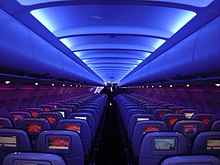
LED lighting in the aircraft cabin of an
Airbus A320 Enhanced.

A large LED display behind a
disc jockey.

LED
destination signs on buses, one with a colored route number.
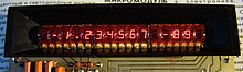
LED digital display that can display 4 digits along with points.
 Traffic light
 using LED
 Western Australia Police
 car with LEDs used in its high-mounted brake light, its
rear window and roof-mounted flashing Police vehicle lights and roof-mounted road user information display.

Printhead of an Oki
LED printer
LED
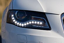
daytime running lights of Audi A4

LED panel light source used in an experiment on
plant growth. The findings of such experiments may be used to grow food in space on long duration missions.
LED Illumination.

LED lights reacting dynamically to video feed via
AmBX.
 Macrophotography
 of an illuminated blue LED
LED uses fall into four major categories:
- Visual signals where light goes more or less directly from the source to the human eye, to convey a message or meaning.
- Illumination where light is reflected from objects to give visual response of these objects.
- Measuring and interacting with processes involving no human vision.[100]
- Narrow band light sensors where LEDs operate in a reverse-bias mode and respond to incident light, instead of emitting light.
For more than 70 years, until the LED, practically all lighting was incandescent and fluorescent with the first fluorescent light only being commercially available after the
1939 World's Fair.
Indicators and signs
The
low energy consumption, low maintenance and small size of modern LEDs has led to uses as status indicators and displays on a variety of equipment and installations. Large-area
LED displays are used as stadium displays and as dynamic decorative displays. Thin, lightweight message displays are used at airports and railway stations, and as
destination displays for trains, buses, trams, and ferries.
One-color light is well suited for
traffic lights and signals,
exit signs,
emergency vehicle lighting, ships' navigation lights or
lanterns (chromacity and luminance standards being set under the Convention on the International Regulations for Preventing Collisions at Sea 1972, Annex I and the CIE) and
LED-based Christmas lights. In cold climates, LED traffic lights may remain snow covered.
[101] Red or yellow LEDs are used in indicator and alphanumeric displays in environments where night vision must be retained: aircraft cockpits, submarine and ship bridges, astronomy observatories, and in the field, e.g. night time animal watching and military field use.
Because of their long life and fast switching times, LEDs have been used in brake lights for cars
high-mounted brake lights, trucks, and buses, and in turn signals for some time, but many vehicles now use LEDs for their rear light clusters. The use in brakes improves safety, due to a great reduction in the time needed to light fully, or faster rise time, up to 0.5 second faster than an incandescent bulb. This gives drivers behind more time to react. It is reported that at normal highway speeds, this equals one car length equivalent in increased time to react. In a dual intensity circuit (i.e., rear markers and brakes) if the LEDs are not pulsed at a fast enough frequency, they can create a
phantom array, where ghost images of the LED will appear if the eyes quickly scan across the array. White LED headlamps are starting to be used. Using LEDs has styling advantages because LEDs can form much thinner lights than incandescent lamps with
parabolic reflectors.
Due to the relative cheapness of low output LEDs, they are also used in many temporary uses such as
glowsticks,
throwies, and the photonic
textile Lumalive. Artists have also used LEDs for
LED art.
Weather/all-hazards radio receivers with
Specific Area Message Encoding (SAME) have three LEDs: red for warnings, orange for watches, and yellow for advisories & statements whenever issued.
Lighting
Main article:
LED lamp
With the development of high efficiency and high power LEDs it has become possible to use LEDs in lighting and illumination. Replacement
light bulbs have been made, as well as dedicated fixtures and
LED lamps. LEDs are used as
street lights and in other
architectural lighting where color changing is used. The mechanical robustness and long lifetime is used in
automotive lighting on cars, motorcycles and on
bicycle lights.
LED street lights are employed on poles and in parking garages. In 2007, the Italian village
Torraca was the first place to convert its entire illumination system to LEDs.
[102]
LEDs are used in
aviation lighting.
Airbus has used LED lighting in their
Airbus A320 Enhanced since 2007, and Boeing plans its use in the
787. LEDs are also being used now in airport and heliport lighting. LED airport fixtures currently include medium-intensity runway lights, runway centerline lights, taxiway centerline & edge lights, guidance signs and obstruction lighting.
LEDs are also suitable for
backlighting for
LCD televisions and lightweight
laptop displays and light source for
DLP projectors (See
LED TV). RGB LEDs raise the color
gamut by as much as 45%. Screens for TV and computer displays can be made thinner using LEDs for backlighting.
[103]
LEDs are used increasingly in aquarium lights. Particularly for reef aquariums, LED lights provide an efficient light source with less heat output to help maintain optimal aquarium temperatures. LED-based aquarium fixtures also have the advantage of being manually adjustable to emit a specific color-spectrum for ideal coloration of corals, fish, and invertebrates while optimizing photosynthetically active radiation (PAR) which raises growth and sustainability of photosynthetic life such as corals, anemones, clams, and macroalgae. These fixtures can be electronically programmed to simulate various lighting conditions throughout the day, reflecting phases of the sun and moon for a dynamic reef experience. LED fixtures typically cost up to five times as much as similarly rated fluorescent or high-intensity discharge lighting designed for reef aquariums and are not as high output to date.
The lack of IR/heat radiation makes LEDs ideal for
stage lights using banks of RGB LEDs that can easily change color and decrease heating from traditional stage lighting, as well as medical lighting where IR-radiation can be harmful. In energy conservation, LEDs lower heat output also means air conditioning(cooling) systems have less heat to dispose of, reducing carbon dioxide emissions.
LEDs are small, durable and need little power, so they are used in hand held devices such as
flashlights. LED
strobe lights or
camera flashes operate at a safe, low voltage, instead of the 250+ volts commonly found in
xenon flashlamp-based lighting. This is especially useful in cameras on
mobile phones, where space is at a premium and bulky voltage-raising circuitry is undesirable.
LEDs are used for infrared illumination in
night vision uses including
security cameras. A ring of LEDs around a
video camera, aimed forward into a
retroreflective background, allows
chroma keying in
video productions.
LEDs are now used commonly in all market areas from commercial to home use: standard lighting and AV installations, stage and theatrical, architectural and public spaces, wherever artificial light is used.
In many countries incandescent lighting for homes and offices is no longer available and building regulations insist on new premises being fitted out at day one with LED fixtures and fittings
[citation needed].
Increasingly the adaptability of color LEDs are finding uses in medical and educational applications such as mood enhancement and new technologies, such as
AmBX, for the control of color LEDs have been developed to exploit LED versatility.
NASA has even sponsored research for the use of LEDs to promote health for astronauts.
[104]
Smart lighting
Light can be used to transmit
broadband data, which is already implemented in
IrDA standards using infrared LEDs. Because LEDs can
cycle on and off millions of times per second, they can be
wireless transmitters and
access points for
data transport.
[105] Lasers can also be
modulated in this manner.
Sustainable lighting
Efficient lighting is needed for
sustainable architecture. In 2009, a typical 13 watt LED lamp emitted 450 to 650 lumens.
[106] which is equivalent to a standard 40 watt incandescent bulb. In 2011, LEDs have become more efficient, so that a 6 Watt LED can easily achieve the same results.
[107] A standard 40 W incandescent bulb has an expected lifespan of 1,000 hours while an LED can continue to operate with reduced efficiency for more than 50,000 hours, 50 times longer than the incandescent bulb.
Energy consumption
One kilowatt-hour of electricity will cause 1.34 pounds (610 g) of CO
2 emission.
[108] Assuming the average light bulb is on for 10 hours a day, one 40-watt incandescent bulb will cause 196 pounds (89 kg) of CO
2 emission per year. The 6-watt LED equivalent will only cause 30 pounds (14 kg) of CO
2 over the same time span. A buildings carbon footprint from lighting can be reduced by 85% by exchanging all incandescent bulbs for new LEDs.
Economically sustainable
LED light bulbs could be a cost-effective option for lighting a home or office space because of their very long lifetimes. Consumer use of LEDs as a replacement for conventional lighting system is currently hampered by the high cost and low efficiency of available products. 2009 DOE testing results showed an average efficacy of 35 lm/W, below that of typical
CFLs, and as low as 9 lm/W, worse than standard incandescents.
[106] However, as of 2011 there are LED bulbs available as efficient as 150 lm/W and even inexpensive low-end models typically exceed 50 lm/W. The high initial cost of the commercial LED bulb is due to the expensive
sapphire substrate which is key to the production process. The sapphire apparatus must be coupled with a mirror-like collector to reflect light that would otherwise be wasted.
Non-visual applications
The light from LEDs can be modulated very quickly so they are used extensively in
optical fiber and
Free Space Optics communications. This include
remote controls, such as for TVs and VCRs, where infrared LEDs are often used.
Opto-isolators use an LED combined with a
photodiode or
phototransistor to provide a signal path with electrical isolation between two circuits. This is especially useful in medical equipment where the signals from a low-voltage
sensor circuit (usually battery powered) in contact with a living organism must be electrically isolated from any possible electrical failure in a recording or monitoring device operating at potentially dangerous voltages. An optoisolator also allows information to be transferred between circuits not sharing a common ground potential.
Many sensor systems rely on light as the signal source. LEDs are often ideal as a light source due to the requirements of the sensors. LEDs are used as
movement sensors, for example in
optical computer mice. The Nintendo
Wii's sensor bar uses infrared LEDs.
Pulse oximeters use them for measuring
oxygen saturation. Some flatbed scanners use arrays of RGB LEDs rather than the typical
cold-cathode fluorescent lamp as the light source. Having independent control of three illuminated colors allows the scanner to calibrate itself for more accurate color balance, and there is no need for warm-up. Further, its sensors only need be monochromatic, since at any one time the page being scanned is only lit by one color of light.
Touch sensing: Since LEDs can also be used as
photodiodes, they can be used for both photo emission and detection. This could be used in for example a touch-sensing screen that register reflected light from a finger or
stylus.
[109]
Many materials and biological systems are sensitive to, or dependent on light.
Grow lights use LEDs to increase
photosynthesis in
plants[110] and bacteria and viruses can be removed from water and other substances using
UV LEDs for
sterilization.
[57] Other uses are as
UV curing devices for some ink and coating methods, and in
LED printers.
Plant growers are interested in LEDs because they are more energy efficient, emit less heat (can damage plants close to hot lamps), and can provide the optimum light frequency for plant growth and bloom periods compared to currently used grow lights:
HPS (high pressure sodium),
MH (metal halide) or
CFL/low-energy. However, LEDs have not replaced these grow lights due to higher price. As mass production and LED kits develop, the LED products will become cheaper.
LEDs have also been used as a medium quality
voltage reference in electronic circuits. The forward voltage drop (e.g., about 1.7 V for a normal red LED) can be used instead of a
Zener diode in low-voltage regulators. Red LEDs have the flattest
I/
V curve above the knee. Nitride-based LEDs have a fairly steep
I/
V curve and are useless for this purpose. Although LED forward voltage is far more current-dependent than a good Zener, Zener diodes are not widely available below voltages of about 3 V.
Light sources for machine vision systems
Machine vision systems often require bright and homogeneous illumination, so features of interest are easier to process. LEDs are often used for this purpose, and this is likely to remain one of their major uses until price drops low enough to make signaling and illumination uses more widespread.
Barcode scanners are the most common example of machine vision, and many low cost ones use red LEDs instead of lasers. Optical computer mice are also another example of LEDs in machine vision, as it is used to provide an even light source on the surface for the miniature camera within the mouse. LEDs constitute a nearly ideal light source for
machine vision systems for several reasons:
The size of the illuminated field is usually comparatively small and machine vision systems are often quite expensive, so the cost of the light source is usually a minor concern. However, it might not be easy to replace a broken light source placed within complex machinery, and here the long service life of LEDs is a benefit.
LED elements tend to be small and can be placed with high density over flat or even-shaped substrates (PCBs etc.) so that bright and homogeneous sources can be designed which direct light from tightly controlled directions on inspected parts. This can often be obtained with small, low-cost lenses and diffusers, helping to achieve high light densities with control over lighting levels and homogeneity. LED sources can be shaped in several configurations (spot lights for reflective illumination; ring lights for coaxial illumination; back lights for contour illumination; linear assemblies; flat, large format panels; dome sources for diffused, omnidirectional illumination).
LEDs can be easily strobed (in the microsecond range and below) and synchronized with imaging. High-power LEDs are available allowing well-lit images even with very short light pulses. This is often used to obtain crisp and sharp still images of quickly moving parts.
LEDs come in several different colors and wavelengths, allowing easy use of the best color for each need, where different color may provide better visibility of features of interest. Having a precisely known spectrum allows tightly matched filters to be used to separate informative bandwidth or to reduce disturbing effects of ambient light. LEDs usually operate at comparatively low working temperatures, simplifying heat management and dissipation. This allows using plastic lenses, filters, and diffusers. Waterproof units can also easily be designed, allowing use in harsh or wet environments (food, beverage, oil industries).
 Electronics portal
 Energy portal
")

 Pin configurationanode and cathode
.svg)


.jpg)


 Electronics portal
 Energy portal

 SS[24] as the HOMO level of this material generally lies between the workfunction of ITO and the HOMO of other commonly used polymers, reducing the energy barriers for hole injection. Metals such as barium and calcium are often used for the cathode as they have low work functions which promote injection of electrons into the LUMO of the organic layer.[25] Such metals are reactive, so require a capping layer of aluminium to avoid degradation.

3.png)


